




Introduction
For years, the AO8801 has been a trusted dual P-channel MOSFET in portable electronics, battery-powered products, and high-side switching circuits. Its compact package and mature design have made it a common choice for engineers developing space-constrained systems. However, today's electronics industry has changed significantly: modern consumer devices are becoming thinner, batteries are expected to last longer, and PCB space is more valuable than ever. At the same time, engineers are under increasing pressure to reduce component count, improve manufacturing efficiency, and simplify layouts.
As a result, many new designs are shifting from traditional discrete or dual P-channel MOSFET solutions toward complementary N+P MOSFETs, which integrate an N-channel and a P-channel MOSFET into a single package. Does this mean the AO8801 is obsolete? Not necessarily. The better question is when you should continue using the AO8801, and when a complementary MOSFET provides a better solution.

Understanding the Technologies
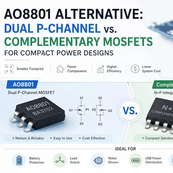
The AO8801 is a dual P-channel enhancement-mode MOSFET that integrates two matched P-channel transistors into one package. Its popularity comes from a mature design, stable supply, small package, low cost, and easy PCB implementation, making it ideal for battery reverse protection, high-side load switching, and portable consumer electronics.
The evolution of compact power switching, however, has driven the adoption of complementary MOSFETs. Several years ago, designers typically built switching circuits using multiple discrete N-channel and P-channel MOSFETs, gate resistors, pull-down resistors, and additional routing. Although flexible, this approach increases PCB size, BOM count, SMT assembly cost, layout complexity, and manufacturing risk. A complementary MOSFET solves this by integrating one N-channel and one P-channel MOSFET inside a single package, giving engineers a smaller PCB footprint, better device matching, lower parasitic inductance, and simpler routing.
AO8801 vs. Complementary MOSFET Comparison
| Evaluation Metric | AO8801 (Dual P-Channel) | Complementary MOSFET (N+P) |
| Structure | Dual P-Channel transistors | Integrated N-Channel and P-Channel pair |
| PCB Area & BOM | Moderate footprint; requires external pull-ups/drivers | Minimized footprint; lower external component count |
| Efficiency & Thermal | Good for high-side switching; standard thermal dissipation | Optimized switching dynamics and lower conduction losses |
| Applications | Simple battery protection, legacy systems, high-side loads | Half-bridge drivers, USB power distribution, smart wearables |
| Cost & Complexity | Low cost, highly mature, straightforward layout | Cost-effective at system level due to reduced BOM count |

When to Choose Each Solution
-
When AO8801 Is Still the Best Choice: Despite newer technologies, the AO8801 continues to perform exceptionally well in simple high-side protection circuits, reverse battery protection for low-cost portable products, legacy product maintenance, and cost-sensitive electronics with stable production volumes. If your design already meets performance targets, redesigning solely for higher integration may not deliver meaningful ROI.
-
When Complementary MOSFETs Are a Better Choice: Complementary MOSFETs shine in modern portable electronics like smartwatches, earbuds, and portable speakers where reducing even a few square millimeters of PCB space frees room for larger batteries. They also simplify battery management systems, small motor drivers (such as camera modules and cooling fans), and USB power distribution accessories by streamlining load switching and power path management.
Key Selection Criteria & Engineering Best Practices
Instead of focusing solely on part numbers or a single parameter like RDS(on), engineers should evaluate a comprehensive set of specifications including drain-to-source voltage, continuous drain current, gate charge, package type, junction temperature, thermal resistance, switching frequency, product lifecycle, and supplier availability. Ignoring factors like gate charge or switching losses can increase manufacturing risk over a product's lifetime.
Furthermore, modern power designs rarely rely on a MOSFET alone. They are typically combined with load switch ICs for current limiting, gate drivers for higher efficiency, battery management ICs for lithium protection, DC/DC converters for voltage regulation, and TVS/ESD protection for system reliability. Selecting these components together simplifies procurement and ensures long-term system compatibility.
Conclusion
The AO8801 remains an excellent dual P-channel MOSFET for many proven designs. However, for new compact electronic products where PCB space, assembly efficiency, and BOM optimization are critical, complementary N+P MOSFETs often provide significant advantages. The best choice depends not only on electrical specifications but also on manufacturability, sourcing stability, and long-term product strategy.


